Dung Rivisions - Custom Eurorack Clone
Introduction
I was lying in bed watching YouTube on my phone when I first came across Rung Divisions by Fancy Synthesis. A clock divider and something like a Turing machine, connected by a bus system, in one module? I wanted it immediately, but I’d already burned through my modular budget for the moment. And when I looked it up on Schneidersladen, it wasn’t available in Germany yet anyway.
In the weeks before, I’d been deep in electronics experiments: microcontrollers, raw components, and random ICs. I knew handling audio on a microcontroller was hard, but clock signals and timing seemed manageable. Then, just days earlier, I’d stumbled across an article about expanding microcontroller I/O with shift registers, and suddenly, it clicked: I could build this myself.
I would have been too intimidated to start from scratch with my own ideas. But building something with an existing module as a model? That felt like the right size of challenge.
Project Start
The first step was to identify all required components and how to source them. It was clear to me that I wanted to build a digital module, as I wanted to build experience there, and also I wanted the result to be able to change the function by uploading different firmwares. I aimed to go as cheap and low-key for the project as possible, so the Arduino Nano was chosen as the brains of the operation.
Quickly it became obvious that I had far too many inputs by all those two-way throw switches and outputs by all the gates and LEDs. So after a quick research, it seemed quite feasible to handle this by using a bunch of 165 and 595 type ICs that are capable of turning parallel data into serial and vice versa. This realization alone made the project worthwhile, as this was one of the great mysteries of the microcontroller world I didn’t grasp yet. The last time I had that kind of epiphany was when I discovered how to build keyboards and such with input matrices.
So then it was just a back and forth about checking required functionality, cross-referencing datasheets, and using AI as a smarter search engine to fill in the gaps to create a rough list of all components required. I decided to use all through-hole components as I already had a lot of them lying around and actually quite enjoy soldering. But maybe that will turn out to be a mistake later.
Though I had this feeling that it would make more sense to create a schematic first, I couldn’t resist and jumped straight to AliExpress for sourcing all the parts. I wanted to know what I will be working with, and I thought it would be good to have the parts ordered so I can do the design and development meanwhile.
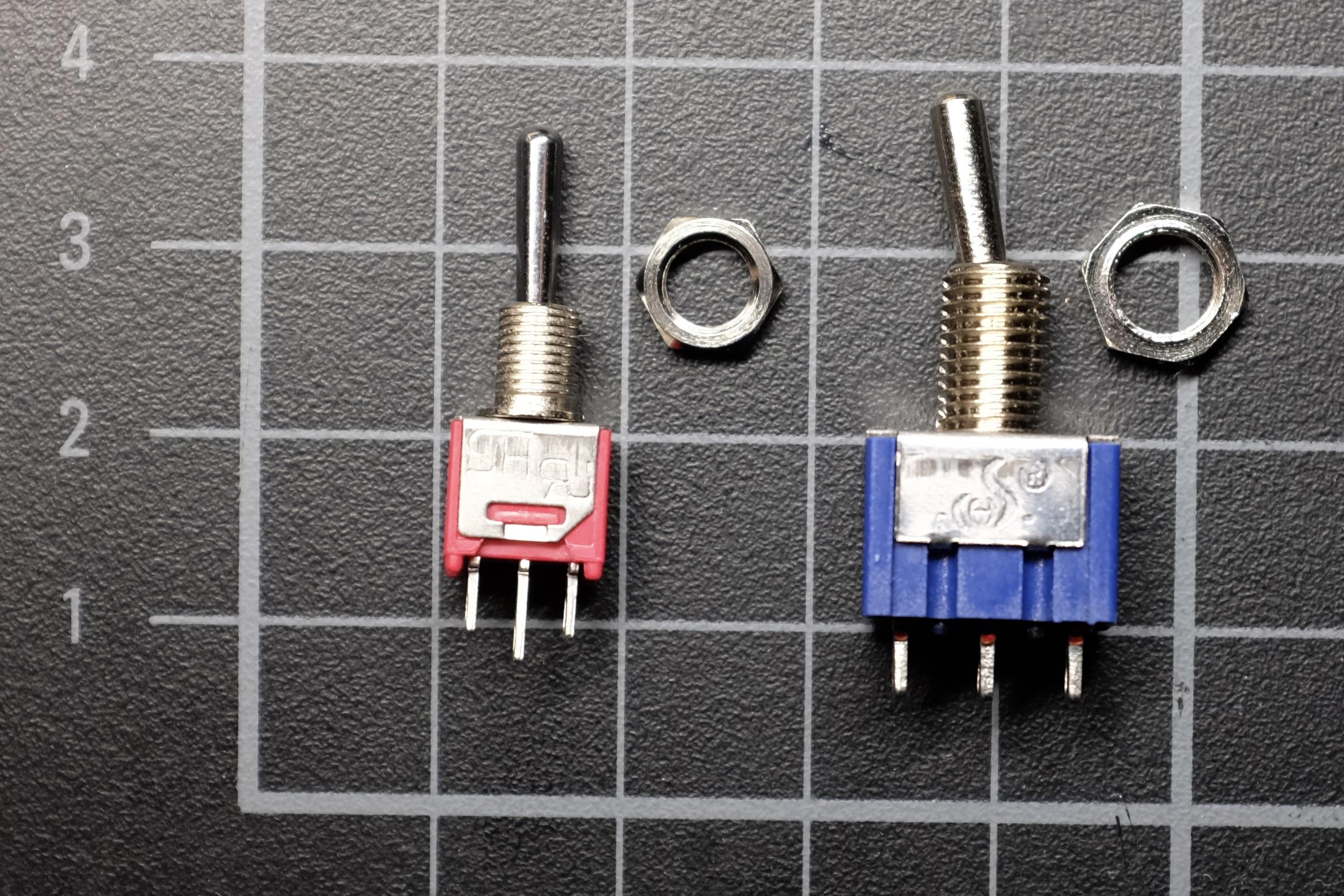
The most difficult part to find was definitely the subminiature throw switches that I saw before on some modules I own. They are almost half the size of the readily available ones on Amazon and such, and it took me quite some time until I was sure I found the right ones.
Now it was time to start creating the schematic and designing the PCBs.
PCB Design
So opening KiCad for the first time was definitely an experience. There are so many different editors, and it was a lot to start with. But having a clear target helps: when you’re not constantly second-guessing design decisions, you can just keep moving. I just followed a YouTube tutorial to get my first components and connections down.
I then just went over all the different sections to complete the module, starting with the power department, over the switch inputs and the connected ICs, up to the outputs and LEDs. It felt like a big puzzle that was continuously taking shape. When there were a bit more complicated parts like voltage dividers and overvoltage protection on the input jacks, I tended over to CircuitLab to verify the setups I came up with were working.
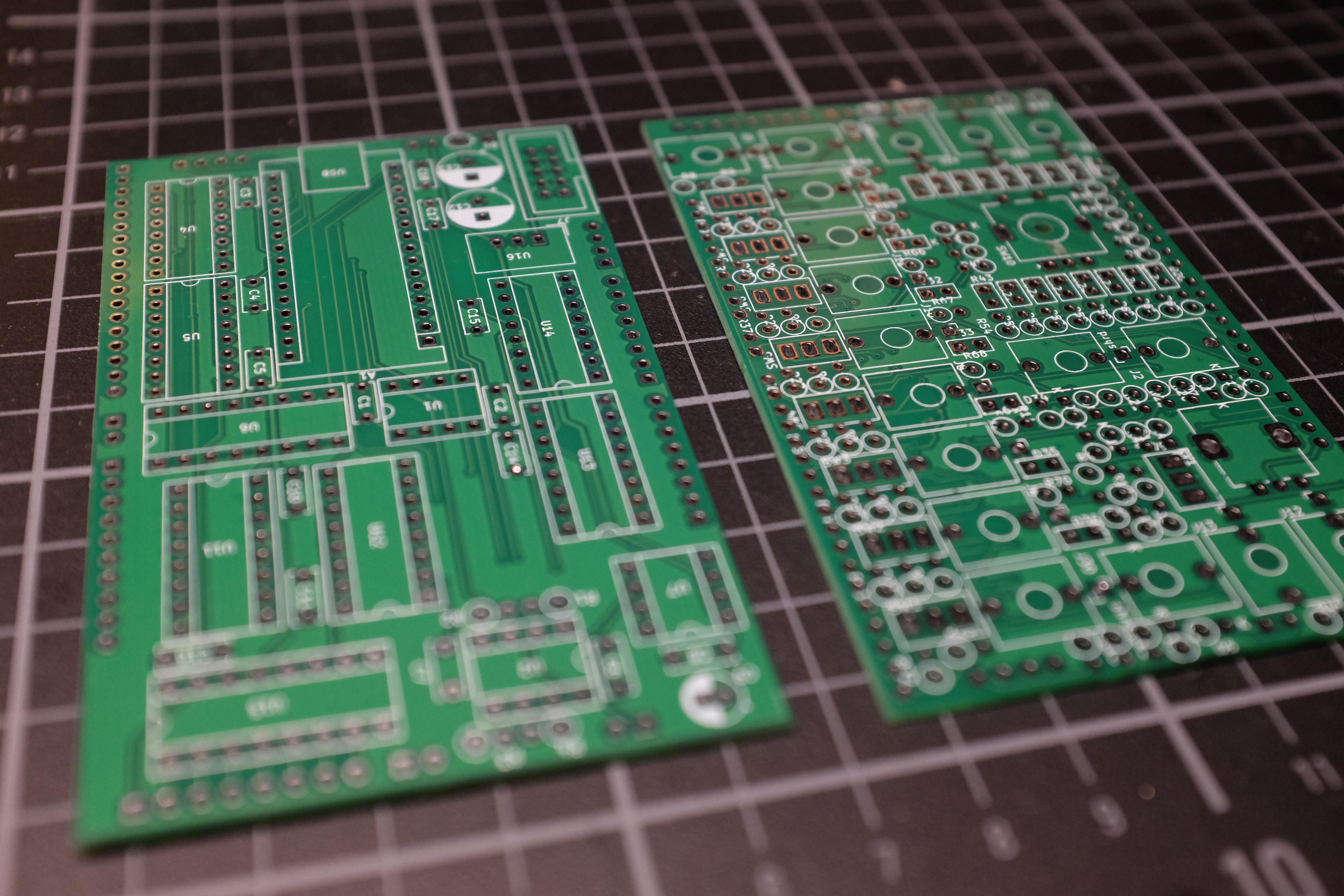
After completing the schematic, I ran into the first big hurdle: I didn’t know the concept of KiCad being one PCB per project. I didn’t really factor this in, and it was clear that I needed a panel PCB for all the interface parts and one for the microcontroller and all the ICs. So after a bit of weighing possibilities, it seemed cleanest to me to just split the projects into two. At least KiCad was so nice here to let me copy and paste the complete arrangement of one schematic into the other.
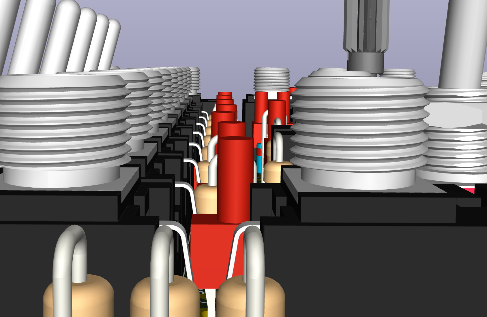
The next shock came right next: I have largely underestimated how many resistors I’ll need and how big through-hole components actually are in numbers. The first import into the PCB-Editor took easily double the space I wanted the module to be, due to the initial margins between components. I was not really hopeful at first, but I just started placing all the interface components first and then painstakingly squeezing all the remaining parts close next to each other. To my own surprise, it worked out in the end with almost no space remaining.

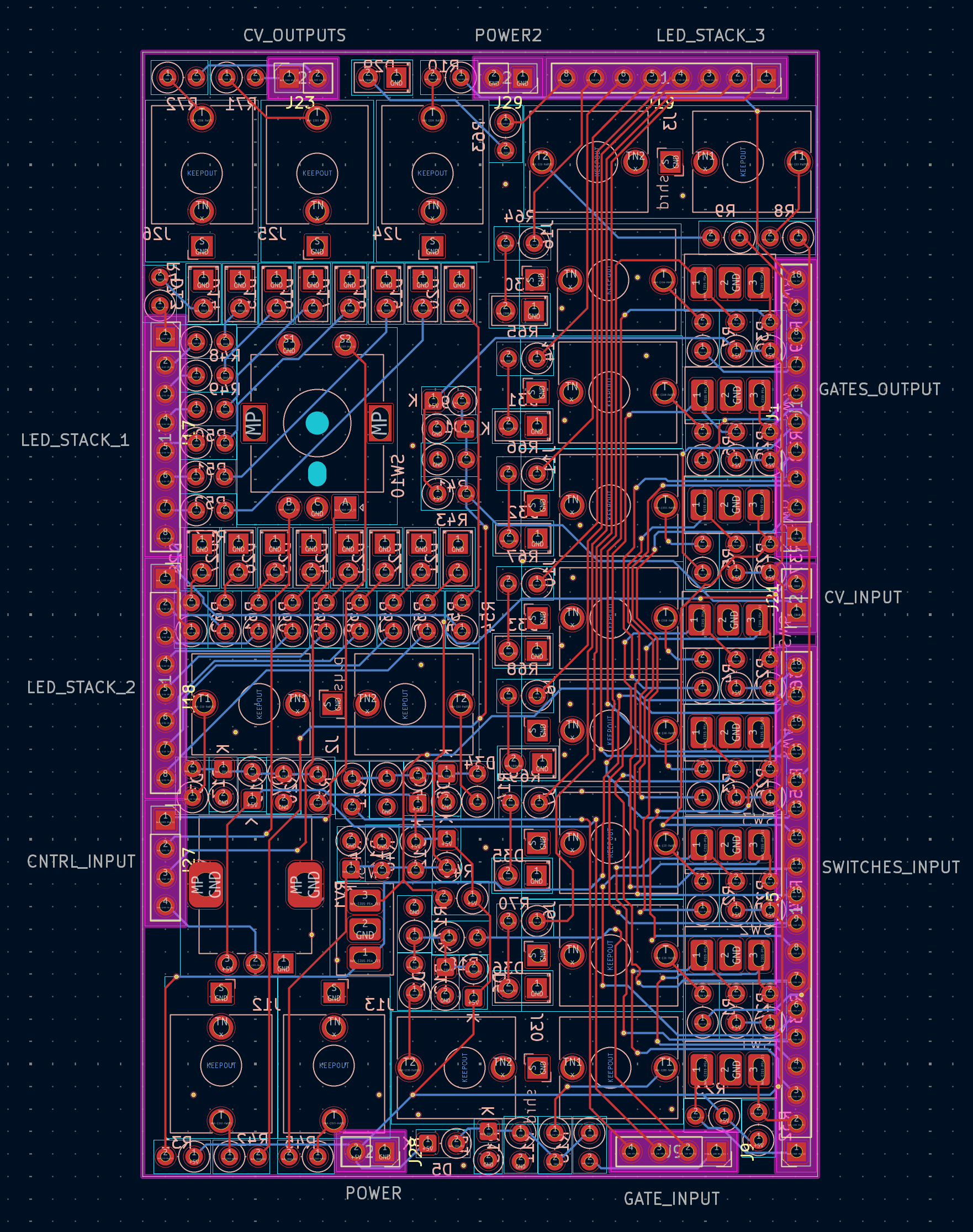
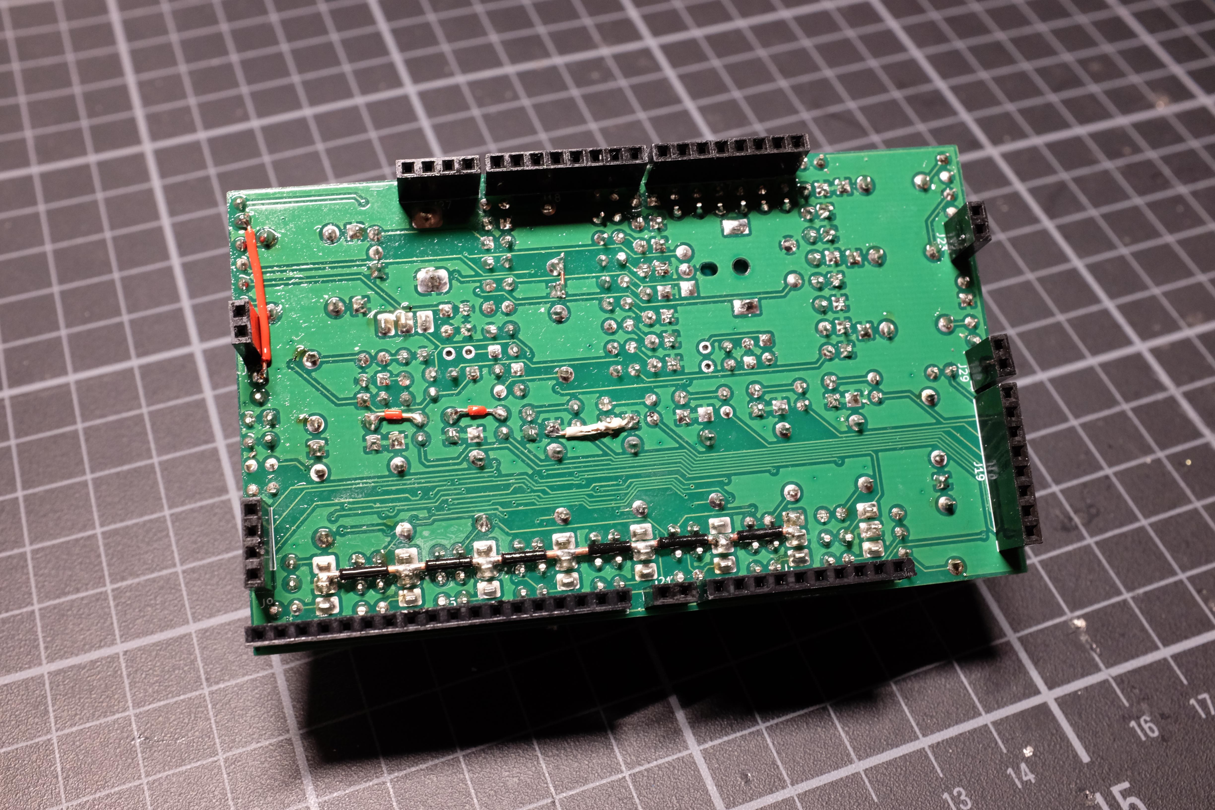
What also felt weird to me at first was the number of connections I needed between my two layers. For some reason, I was expecting the ICs to also fit on the panel layer, but that was quickly unfeasible. So I had to route all the parallel lines, which resulted in somewhere around 60 connections needing to be made. But also here, I was just holding on to the thought that at least I have a solution to do it by just filling all the edges with pin headers and sockets and seeing how it goes.
Now with the project completed, I saw similar design choices on other modules I have, making me a little bit more relaxed regarding that.
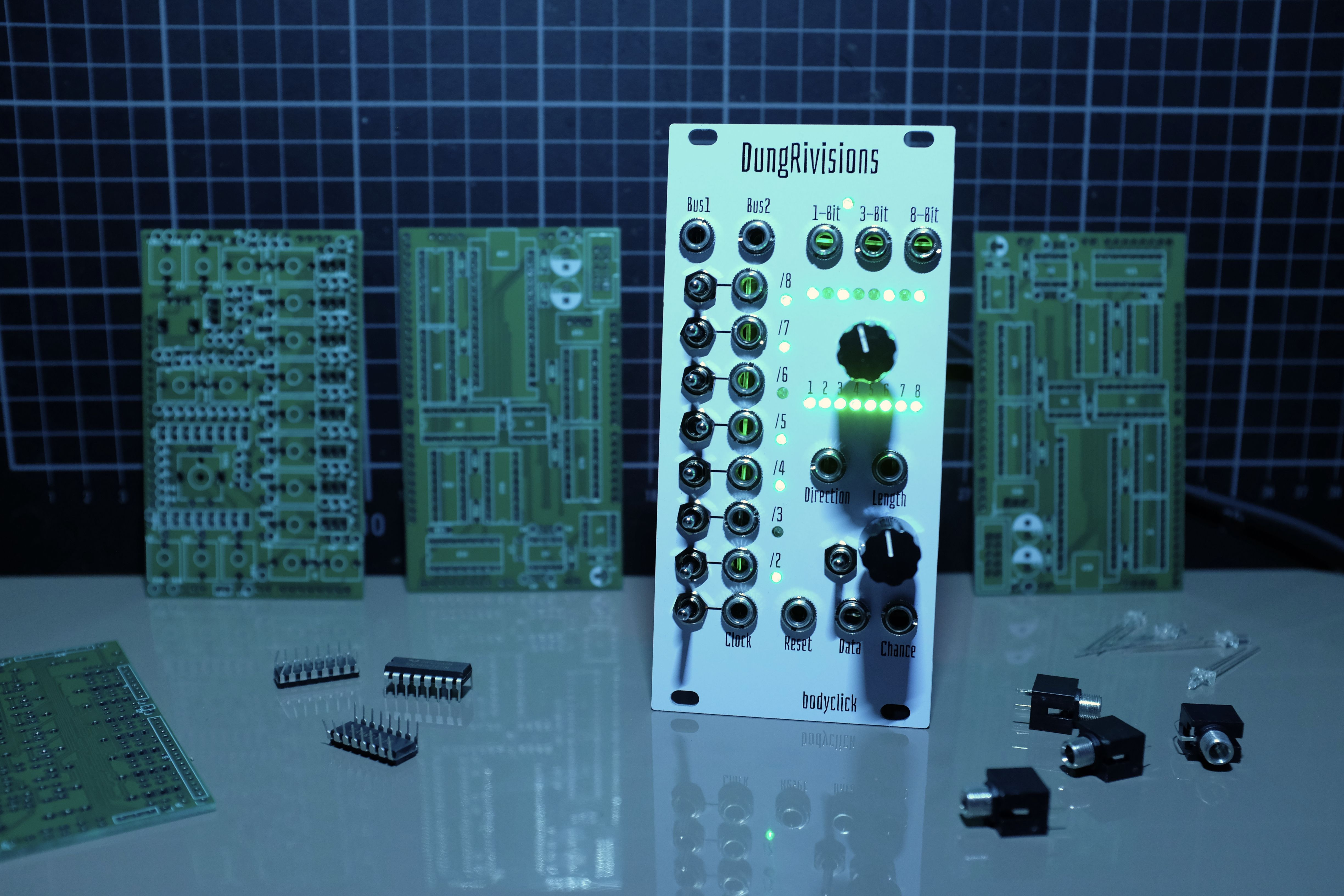
So in the end I needed to ignore a lot of KiCad’s overlapping and placement errors to get it all positioned, and I was also faced with consequences of not aiming for perfect alignment. Jacks, LEDs and buttons were aligned by eye, but at some perspectives in the 3D view, it looked really skewed. But I was pretty sure that those components would have a bit of play later and would nicely sort themselves by mounting on a faceplate before soldering. Spoiler: That worked out really great!
Software
Before starting head first into developing software, I knew I wanted a more sophisticated project setup, enabling me to test the logic part quickly on my computer. A reason for that could be that I didn’t have the hardware yet, but much more important was the fact that I dislike debugging on embedded hardware when it is not necessary. Pushing firmware is slow, and it just doesn’t feel right to do it often. And coming from the cosy world of hot-reload web development, I am addicted to seeing my changes instantly.
So the first task was to set up this dual environment thing. PlatformIO is a great next step after outgrowing the Arduino IDE, mainly because you can work in Visual Studio Code with IntelliSense support and importantly here for having multiple deployment targets. So the core structure was to have the logic part encapsulated away from any actual hardware code. To facilitate that, I introduced a hardware interface, after which an implementation for both targets was created.
rung-divisions/
├── lib/
│   └── rung-divisions/
│       ├── IHardware.h
│       ├── RungDivisions.h
│       └── RungDivisions.cpp
├── src/
│   ├── main.cpp
│   ├── HardwareArduino.h
│   ├── HardwareArduino.cpp
│   ├── HardwareMock.h
│   └── HardwareMock.cpp
└── platformio.ini
There was a vision of having a graphical user interface and seeing the module on the screen, but to keep complexity low I stuck to text output on the command line. After the initial setup was proven to work, I scrambled together a file watcher that automatically compiled and executed the code. That seemed like the most bang for the buck here and worked out pretty well. I think this was the first time I really enjoyed developing for a microcontroller.
It was really uncertain how long this would take, but roughly after just two days I marked the software - at least the logic part - as feature complete. Everything I was deducting from the original module was implemented and seemed working. Now it was time for taking a break while waiting for the components to arrive.
First Assembly
I waited about 2 weeks for my PCBs to arrive, the components came a bit quicker. At first, I didn’t really know what to do and thought it would be a good idea to check some basic ground and power connections on the boards first. That turned out to be a good first call, as already here I discovered a few missing connections that I overlooked in my stuffed design. After noting those, I continued by finally soldering the first module.
It took a while, as I was working directly with the KiCad Schematics and PCB Editor, always manually highlighting the current set of components I was dealing with. Only later, for the next two assemblies, did I discover this great HTML BOM plugin, which creates an interactive document where you can just hover over one component in the list or directly on the PCB drawing and can see instantly what it is and where else it appears. A real timesaver right there.
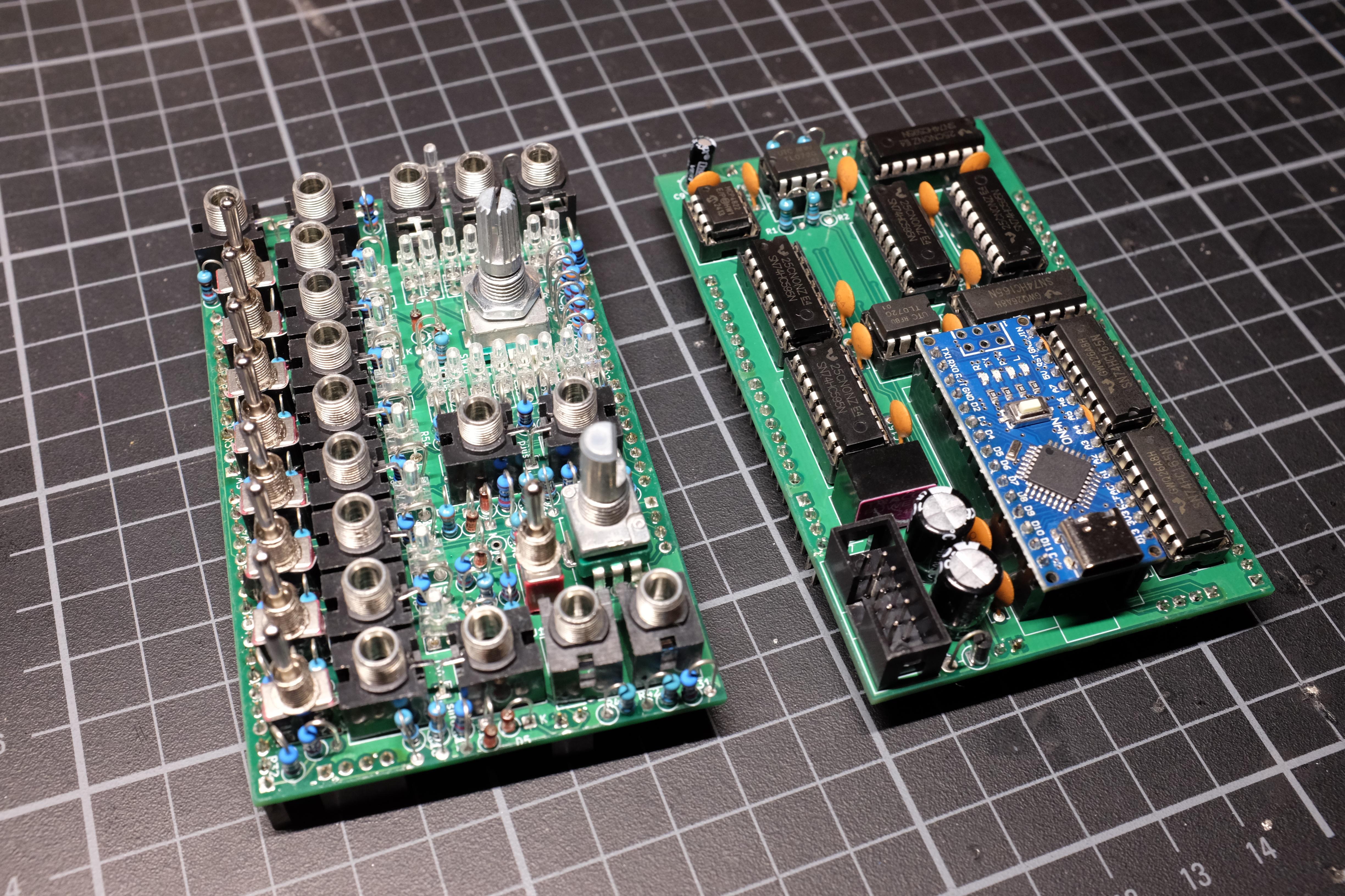
So after completing the first build, I was really nervous about plugging it in and throwing some firmware on it. I had confirmed before that it at least compiles, but this was the real deal now! And to my own surprise, it worked! At least some LEDs were flashing and things were happening. Nothing really terrible happened.
So next I wrote some small test scripts to verify all inputs and outputs are working as expected. Here I was confronted again with my decision to route the components with a focus on straight paths over order, and in the end I got it working with mapping tables for all the shift register chips.
Then I discovered only two more missed connections, and the actual first module was complete! I deployed the actual firmware, tested it as a whole and discovered some more minor bugs or weird behaviours due to the hardware or the software now actually running on a loop, where before it just ran for a fixed number of steps.
It took a few days to fix and tweak, but then I was actually at a point where I was pleased with the result. It went so far over my expectations that I really wanted to get proper front panels fabricated next.
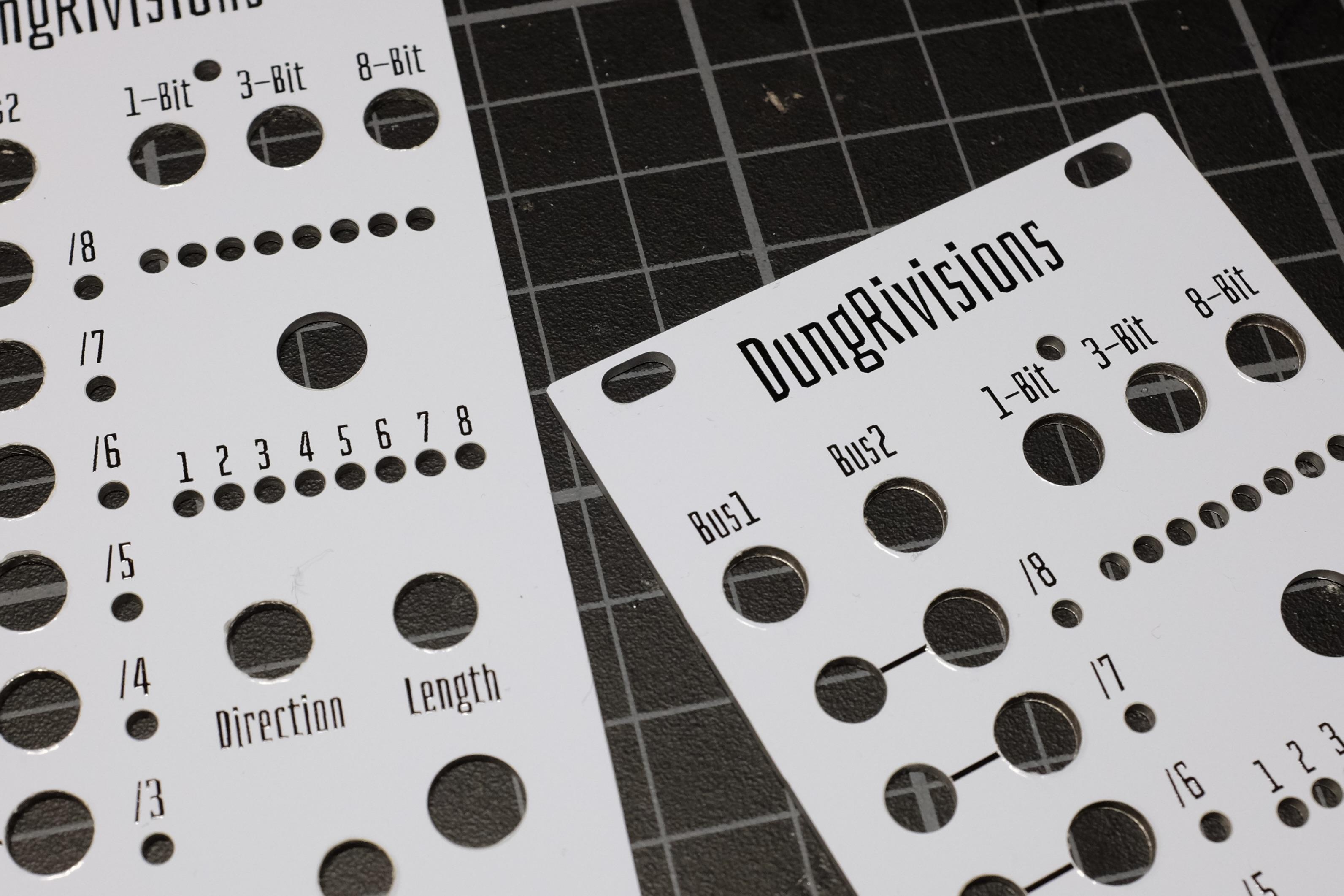
Front Panels
At first, I planned to order my front panels as a sheet metal fabrication at JLCCNC. There are some nice options with powder coating as a finish, which I expected to look fabulous. But for that also, the price would be fabulous in its own right. So after some researching and weighing in the options, I actually ended up ordering aluminium core PCBs.
They are dirt cheap, and I thought already having managed to order full-fledged PCBs could give me a head start here because the instructions on sheet metal data were confusing to me.
But still, it turned out as quite the journey. In the end, I exported flat SVG files from my FreeCAD model and placed them on the EdgeCuts Layer in KiCad. Next I imported this same SVG into Figma, as this was the design tool I felt the most comfortable getting all my texts and markings aligned in an acceptable fashion. I chose the somewhat funny Bahianita font for its cool character while staying relatively readable in smaller sizes. Then I flattened the texts to raw paths and imported all those to the Silkscreen Layer back in KiCad.
Looking now back on it makes it seem almost easy, but it really took some trial and error to get here. At this point, my 3D Rendering in KiCad looked perfect, and I felt ready to upload to the fabricator. And here I got a small bump in hope, as the holes weren’t rendered at all in the preview. At that moment I was tired, it was already late, and I figured I’d just order and hope for the best.
And oh boy did they deliver! After another ten days, the panels arrived and absolutely blew me away. The cutouts were clean, and the Silkscreen was totally crisp. I had read some criticism about this process, but I was totally stunned by the result. The panel fitted on like a glove and at this point I really felt that this project was finished.
Conclusion
This was a really cool project, and I’m so happy that I embarked on it. I really wanted to get into building modules, and by taking away the nagging question of what to make the steps seem a bit more manageable.
I faced some really difficult challenges and was overwhelmed occasionally, but that initial spark, that moment where I actually understood how everything will work together, carried me through the whole process.
Furthermore, I wish I tried to push the design on the panels a little bit further, to have some negative parts and more graphical elements overall, like the Make Noise Or Noise Engineering Modules have. But for the first try, this went really well!
Overall, it took me roughly a whole month, including the wait for parts to arrive. And by usage of cheap parts, the raw hardware cost of a finished module stayed under 40€. So for me that was a full success, and I’m really looking forward to ideating my own module next.